Coplanarity Detection in the Semiconductor Industry: Applications, Prospects, and Trends
Coplanarity Detection in the Semiconductor Industry: Applications, Prospects, and Trends
Coplanarity detection, a critical process for ensuring points, lines, or surfaces lie on the same plane, plays a pivotal role in the semiconductor industry. It directly impacts product quality, process precision, and production efficiency. This article explores its applications, development prospects, and future trends in the semiconductor sector, offering insights for industry professionals.
Applications of Coplanarity Detection in the Semiconductor Industry
Key Applications
Coplanarity detection ensures precision in various semiconductor manufacturing processes. Its primary applications include:
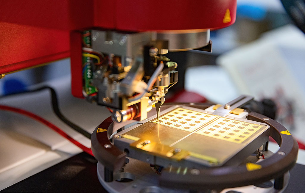
- Wafer Fabrication
Wafer surface flatness (coplanarity) is crucial for photolithography accuracy. Minor height variations can cause defocusing of lithographic patterns, reducing chip yield.
Example: TSMC employs high-precision laser interferometers and atomic force microscopes (AFM) to ensure nanoscale wafer flatness in 5nm and smaller nodes. - Chip Packaging
In flip-chip or 3D stacked packaging, coplanarity detection verifies chip-to-substrate alignment, ensuring reliable solder joint connections (e.g., BGA or micro-bumps).
Example: Intel uses 3D optical scanning to check substrate and chip flatness in Meteor Lake packaging. - Printed Circuit Board (PCB) Manufacturing
PCB surface coplanarity ensures accurate placement of surface-mount devices (SMDs) and reliable soldering, preventing poor contacts or short circuits.
Example: Foxconn integrates automated optical inspection (AOI) with laser measurement to monitor multilayer PCB flatness. - Display Panel Production
In OLED and LCD panel manufacturing, coplanarity detection ensures glass or flexible substrates are flat, maintaining pixel alignment and display uniformity.
Example: Samsung Display leverages structured light technology to verify AMOLED substrate flatness.
Why It Matters
Coplanarity detection is essential for achieving nanoscale precision, improving yield, and supporting advanced semiconductor technologies like 3D integration.
Development Prospects in the Semiconductor Industry
Growth Drivers
- Demand for Ultra-Precision: As chip nodes shrink to 3nm and below, coplanarity requirements reach sub-nanometer levels, driving innovation in detection equipment.
- Automation and Intelligence: Semiconductor factories are transitioning to full automation, with AI-integrated coplanarity detection systems enabling real-time data analysis and process optimization.
- Market Growth: The global semiconductor market, projected to exceed $600 billion in 2024, fuels demand for quality control technologies like coplanarity detection.
- Equipment Miniaturization: Portable detection tools, such as handheld laser scanners, are making technology accessible to small and medium-sized enterprises, reducing costs.
Future Trends
- Multimodal Detection: Combining optical, X-ray, and ultrasonic technologies will enhance coplanarity analysis for complex 3D packaging structures.
- AI and Big Data Integration: Cloud-based analytics will predict wafer defects and optimize production parameters. For instance, ASML is developing AI-driven wafer flatness prediction models.
- Green Technology: Low-power detection equipment and recyclable materials align with the semiconductor industry’s sustainability goals.
- Real-Time In-Line Detection: Future systems will embed coplanarity monitoring into production lines, enabling real-time wafer and packaging analysis with shorter feedback cycles.
Industry Trends and Challenges
Emerging Trends
- Precision and Efficiency: The semiconductor industry demands detection equipment that delivers nanoscale accuracy at high throughput to meet production needs.
- AI and Automation Synergy: AI-driven systems will enable adaptive calibration and defect prediction, significantly improving detection efficiency.
- Multisensor Integration: Combining optical, laser, and ultrasonic technologies will create versatile multimodal detection systems for complex structures and materials.
- Data-Driven Optimization: Detection data integrated with cloud-based digital twin platforms will enhance process optimization and predictive maintenance.
Key Challenges
- Cost and Accessibility: High-precision detection equipment is costly, posing barriers for smaller firms. Affordable solutions are needed to broaden adoption.
- Complex Material Compatibility: Flexible substrates and heterogeneous integration demand advanced detection techniques.
- Data Privacy and Security: Cloud-based detection requires robust encryption to protect proprietary process data.
- Lack of Standardization: Non-unified equipment standards across vendors can lead to data compatibility issues.
Conclusion
In the semiconductor industry, coplanarity detection is a cornerstone of wafer fabrication, chip packaging, and PCB production. As the industry advances toward 3nm nodes and 3D packaging, detection technologies will evolve toward multimodal, intelligent, and sustainable solutions. Despite challenges like high costs, complex materials, and standardization gaps, advancements in AI, automation, and multisensor systems will drive progress. With the global semiconductor market poised for continued growth, coplanarity detection is set to remain a critical enabler of smart manufacturing.
For more insights into coplanarity detection or semiconductor trends, explore our resources or contact us today!