AI and Automated Equipment in Semiconductor Defect Detection and Electronics Manufacturing Optimization
Introduction
Semiconductor manufacturing and electronics production are highly precise and complex industrial processes where even minor defects can lead to performance degradation or failure. Traditional manual inspection methods are inefficient, costly, and struggle to meet the demands of modern high-precision manufacturing. With the rapid advancement of artificial intelligence (AI) and automated inspection equipment, the semiconductor industry is undergoing an intelligent transformation. AI combined with advanced machinery not only enhances defect detection but also optimizes production workflows, improving yield rates and reducing costs. This article explores the applications of AI and automated equipment in semiconductor defect detection and electronics manufacturing optimization.
1. Challenges in Semiconductor Defect Detection
Semiconductor manufacturing involves multiple stages, including lithography, etching, deposition, and packaging, each susceptible to defects such as:
-
Particle contamination – Tiny particles adhering to wafers, affecting circuit performance.
-
Uneven etching – Leading to short circuits or open circuits.
-
Metal layer misalignment – Impacting chip conductivity.
-
Packaging defects – Such as poor soldering or warping.
Traditional inspection methods (e.g., optical microscopy, electron microscopy) rely on manual visual checks, which are slow and subjective. AI-powered automated systems significantly improve detection speed and accuracy.
2. AI Applications in Semiconductor Defect Detection
2.1 Deep Learning-Based Visual Inspection
AI vision systems use convolutional neural networks (CNNs) to identify defect patterns, offering:
-
High-precision detection – Identifies micron-level defects like scratches or contamination.
-
Real-time analysis – High-speed cameras enable inline defect screening.
-
Adaptive learning – AI models continuously improve, reducing false positives.
For example, TSMC’s AI vision system increased wafer defect detection speed by 50% while lowering false rejection rates by 30%.
2.2 Acoustic and Infrared Inspection
Beyond visual inspection, AI integrates with:
-
Ultrasonic testing – Detects internal voids or cracks in packaging.
-
Infrared thermography – Identifies abnormal chip heating, predicting failure risks.
AI analyzes acoustic or thermal signals to pinpoint defects without destructive testing.
2.3 Big Data & Predictive Maintenance
AI processes vast semiconductor production data to:
-
Monitor equipment health – Predicts failures using vibration, temperature, and other sensor data.
-
Optimize processes – Identifies key parameters (temperature, humidity, gas flow) affecting yield and adjusts them automatically.
3. Automated Equipment in Defect Detection
3.1 Automated Optical Inspection (AOI) Systems
AOI combines high-resolution cameras with AI to scan PCBs and wafers, detecting:
-
Solder defects (cold joints, bridging)
-
Broken or shorted circuits
-
Misplaced or missing components
Samsung’s AOI system improved PCB inspection efficiency by 70% while reducing manual rechecks by 60%.
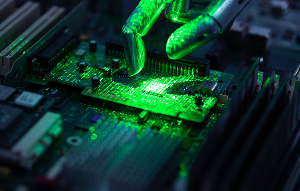
3.2 Robotic Inspection & Sorting
Industrial robots with AI vision enable:
-
Automatic defect sorting – Robotic arms remove faulty products from the line.
-
Micron-level precision – Robots perform stable chip placement and soldering.
3.3 3D X-Ray Inspection
For advanced packaging (e.g., 5G chips, HBM memory), AI-enhanced 3D X-ray provides non-destructive detection of:
-
Internal solder joint quality
-
Through-silicon via (TSV) connections
-
Delamination in packaging layers
4. AI & Automation in Electronics Production Optimization
4.1 Smart Process Control
AI dynamically adjusts manufacturing parameters, such as:
-
Lithography optimization – Adjusts exposure energy based on wafer surface conditions.
-
Etching endpoint detection – Monitors etching rates in real time to prevent over/under-etching.
4.2 Digital Twin & Virtual Commissioning
Digital Twin technology simulates production lines, allowing AI to optimize:
-
Equipment layout
-
Material flow efficiency
-
Energy consumption
Intel reduced new production line setup time by 40% using Digital Twin simulations.
4.3 Supply Chain & Inventory Optimization
AI forecasts demand to optimize:
-
Raw material procurement
-
Inventory management
-
Mitigates chip shortages
5. Future Trends
-
Lightweight AI models – Enable real-time edge computing for localized inspections.
-
AI + quantum sensing – Enhances nanoscale defect detection.
-
Fully automated smart factories – AI-driven “lights-out” manufacturing with minimal human intervention.
Conclusion
The integration of AI and automated inspection equipment is revolutionizing semiconductor and electronics manufacturing. AI enhances defect detection, optimizes production, and reduces costs. As AI technology advances, smart manufacturing will achieve greater automation and intelligence, driving the next evolution of the electronics industry.